Q1 MHT CET 2026 · 14 MAY · SHIFT 1 Easy ☆
P-N Junction Diode
In the middle of the depletion region of reversed biased p-n junction the
(a) electric field is zero (b) potential is infinite (c) electric field is maximum (d) potential is zero Show answer and solution
Answer: (c)
Loading the solution…
Report a mistake Q2 MHT CET 2026 · 20 APR · SHIFT 2 Easy ☆
P-N Junction Diode
The depletion region of p-n junction
(a) increases if reverse biased. (b) increases if forward biased. (c) decreases if reverse biased. (d) remains same in reverse and forward biasing. Show answer and solution
Answer: (a)
Loading the solution…
Report a mistake Q3 MHT CET 2026 · 13 MAY · SHIFT 2 Easy ☆
P-N Junction Diode
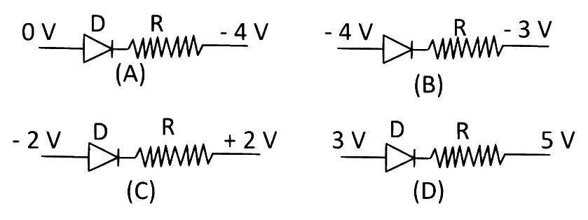
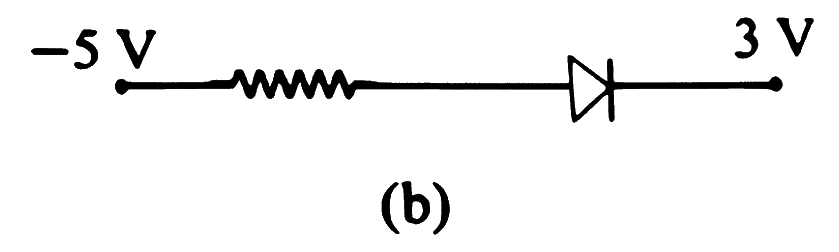
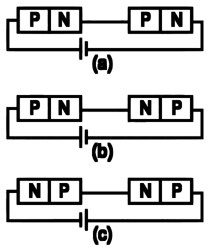
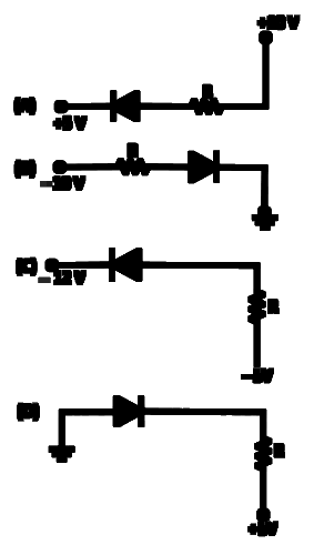
The forward biased diode connection is
Show answer and solution
Answer: (a)
Loading the solution…
Report a mistake Q4 MHT CET 2026 · 18 APR · SHIFT 1 Easy ☆
P-N Junction Diode
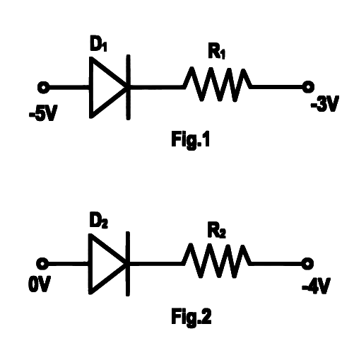
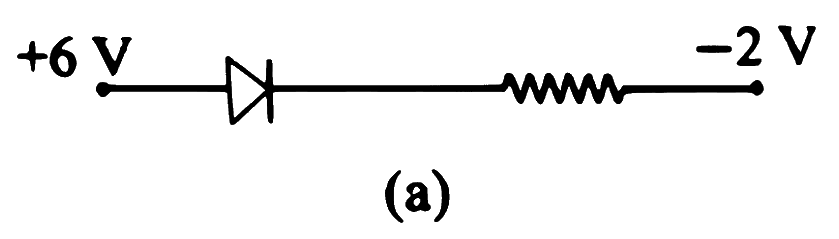
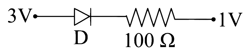
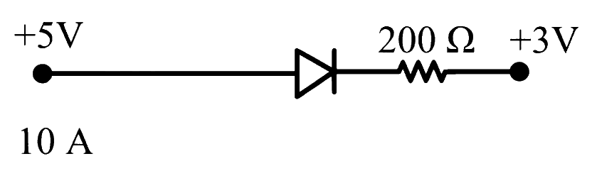
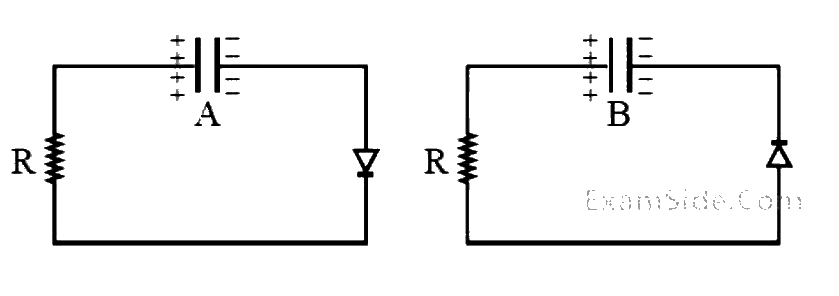
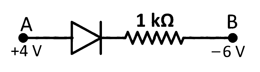
A diode and resistance are connected as shown in figures.
Out of the following statements, which one is true?
Diode in
A) fig (1) and fig (2) are both forward biased.
B) fig (1) and fig (2) are both reverse biased.
C) fig (1) is forward biased and in fig (2) is reverse biased.
D) fig (1) is reverse biased and in fig (2) is forward biased.
Show answer and solution
Answer: (a)
Loading the solution…
Report a mistake Q5 MHT CET 2026 · 15 APR · SHIFT 1 Easy ☆
P-N Junction Diode
For a p-n junction diode, breakdown voltage occurs when
(a) reverse bias is decreased (b) reverse bias is not changed (c) reverse-bias is increased (d) forward bias is increased Show answer and solution
Answer: (c)
Loading the solution…
Report a mistake Q6 MHT CET 2026 · 15 APR · SHIFT 1 Easy ☆
P-N Junction Diode
If p-n junction diode is forward biased then
(a) width of depletion layer decreases. (b) width of depletion layer increases. (c) barrier voltage increases (d) electric conduction is not possible Show answer and solution
Answer: (a)
Loading the solution…
Report a mistake Q7 NEET 2026 Easy ☆
P-N Junction Diode
Two statements are given below:
A. When the forward bias voltage across a p-n junction diode increases above a certain threshold voltage, the diode current increases significantly.
B. This current is called reverse saturation current.
Choose the correct answer from the options given below:
(a) Both Statements A and B are true (b) Statement A is true, but Statement B is false (c) Both Statements A A A B B B (d) Statement A is false, but Statement B is true Show answer and solution
Answer: (b)
Loading the solution…
Report a mistake Q8 JEE Main 2026 · 5 APR · SHIFT 2 Medium ☆
P-N Junction Diode
In a semiconductor p p p p p p n n n 1 0 15 10^{15} 1 0 15 / cm 3 /\text{cm}^{3} / cm 3 1 0 18 10^{18} 1 0 18 / cm 3 /\text{cm}^{3} / cm 3
(a) Widths of depletion region on either side of the interface are equal (b) The depletion region width is more on p -side compared to that in n -side (c) The depletion region width is more on n n n p p p (d) No depletion region forms because of unequal doping concentrations on p and n -sides Show answer and solution
Answer: (b)
Loading the solution…
Report a mistake Q9 MHT CET 2026 · 17 APR · SHIFT 2 Medium ☆
P-N Junction Diode
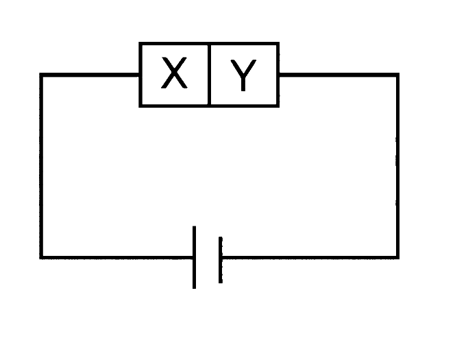
A semiconductor X is made by doping a germanium crystal with indium ( Z = 49 ) (Z = 49) ( Z = 49 ) ( Z = 33 ) (Z = 33) ( Z = 33 )
(a) X is p-type, Y is n-type and the junction is forward biased. (b) X is p-type, Y is n-type and the junction is reverse biased. (c) X is n-type, Y is p-type and the junction is forward biased. (d) X is n-type, Y is p-type and the junction is reverse biased. Show answer and solution
Answer: (a)
Loading the solution…
Report a mistake Q10 NEET 2026 · RE-NEET Medium ☆
P-N Junction Diode
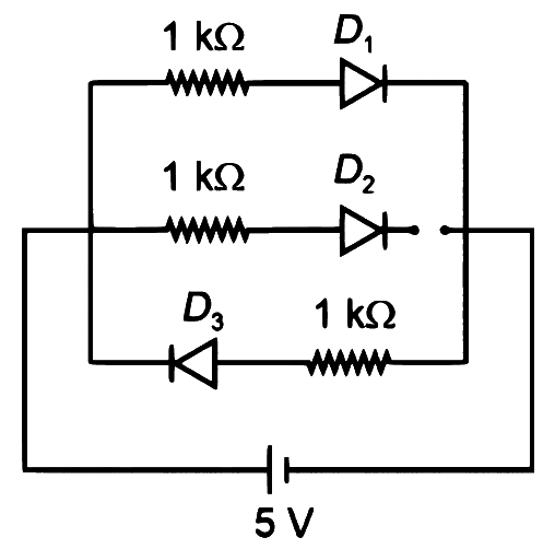
Three identical p-n junction diodes D 1 , D 2 D_1, D_2 D 1 , D 2 D 3 D_3 D 3 D 1 , D 2 D_1, D_2 D 1 , D 2 D 3 D_3 D 3 W 1 , W 2 W_1, W_2 W 1 , W 2 W 3 W_3 W 3
(a) W 2 > W 1 = W 3 W_2 > W_1 = W_3 W 2 > W 1 = W 3 (b) W 1 > W 2 > W 3 W_1 > W_2 > W_3 W 1 > W 2 > W 3 (c) W 3 = W 1 > W 2 W_3 = W_1 > W_2 W 3 = W 1 > W 2 (d) W 3 > W 2 > W 1 W_3 > W_2 > W_1 W 3 > W 2 > W 1 Show answer and solution
Answer: (d)
Loading the solution…
Report a mistake Q11 JEE Main 2026 · 4 APR · SHIFT 2 Medium ☆
P-N Junction Diode
Given below are two statements: one is labelled as Assertion A and the other is labelled as Reason R \mathbf{R} R
Assertion A: A diode under reverse-biased condition provides very small current which is nearly independent of voltage until a critical limit at which the current increases drastically. Reason R: Below the critical voltage limit, only majority charge carriers flow which increases drastically above critical voltage.
choose the correct answer from the options given below
(a) Both A \mathbf{A} A R \mathbf{R} R R \mathbf{R} R A \mathbf{A} A (b) Both A \mathbf{A} A R \mathbf{R} R R \mathbf{R} R A \mathbf{A} A (c) A is true but R \mathbf{R} R (d) A is false but R \mathbf{R} R Show answer and solution
Answer: (c)
Loading the solution…
Report a mistake Q12 MHT CET 2026 · 12 MAY · SHIFT 2 Medium ☆
P-N Junction Diode
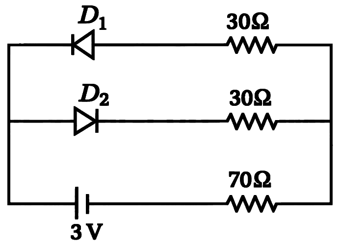
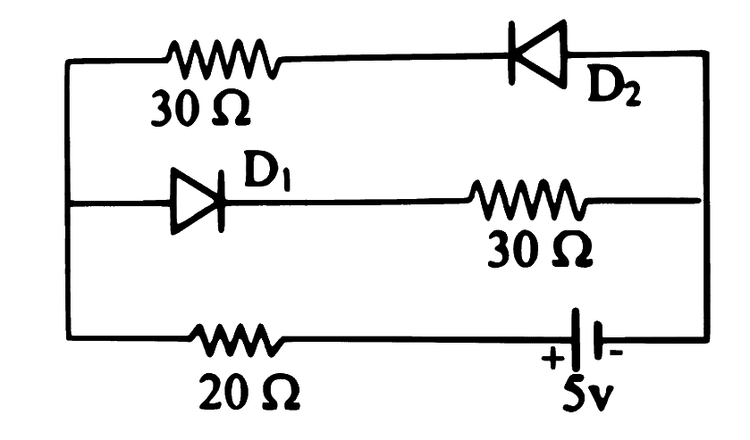
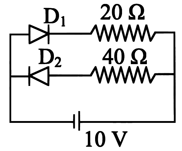
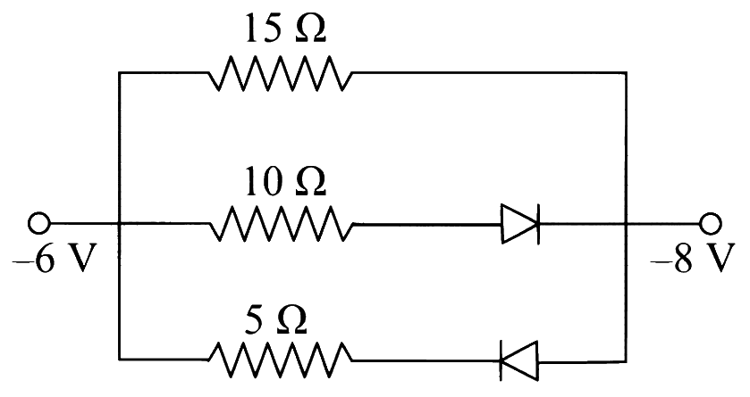
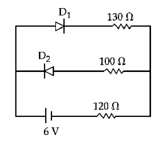
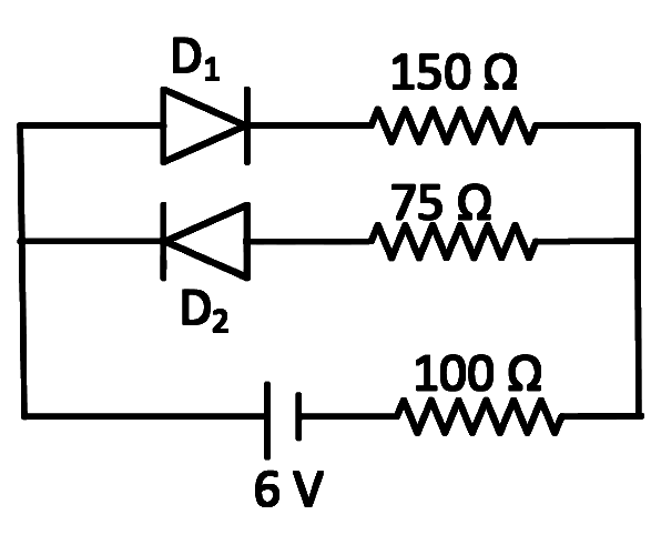
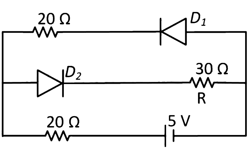
The circuit shown contains two ideal diodes D 1 D_1 D 1 D 2 D_2 D 2 3 3 3 70 Ω 70\ \Omega 70 Ω
(a) 0.01 0.01 0.01 (b) 0.02 0.02 0.02 (c) 0.03 0.03 0.03 (d) 0 0 0 Show answer and solution
Answer: (c)
Loading the solution…
Report a mistake Q13 MHT CET 2026 · 12 MAY · SHIFT 1 Medium ☆
P-N Junction Diode
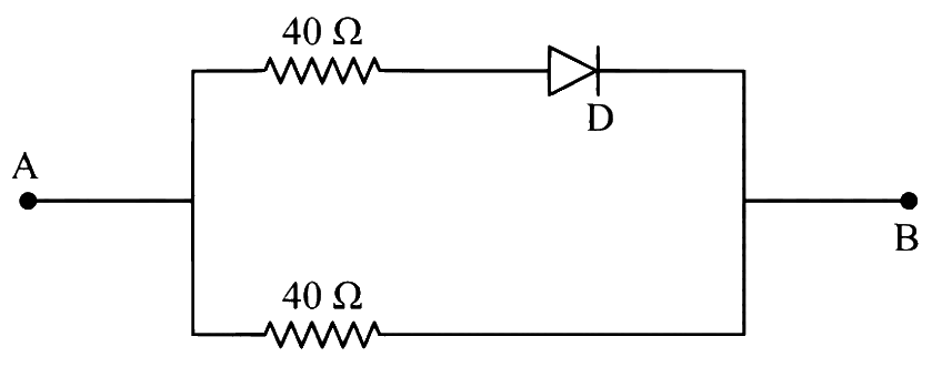
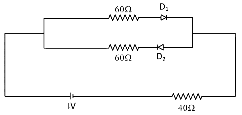
In one branch, 40 Ω 40\ \Omega 40 Ω 40 Ω 40\ \Omega 40 Ω
(a) 40 Ω 40\ \Omega 40 Ω 20 Ω 20\ \Omega 20 Ω (b) 60 Ω 60\ \Omega 60 Ω 30 Ω 30\ \Omega 30 Ω (c) 20 Ω 20\ \Omega 20 Ω 40 Ω 40\ \Omega 40 Ω (d) 30 Ω 30\ \Omega 30 Ω 60 Ω 60\ \Omega 60 Ω Show answer and solution
Answer: (c)
Loading the solution…
Report a mistake Q14 MHT CET 2026 · 19 APR · SHIFT 2 Medium ☆
P-N Junction Diode
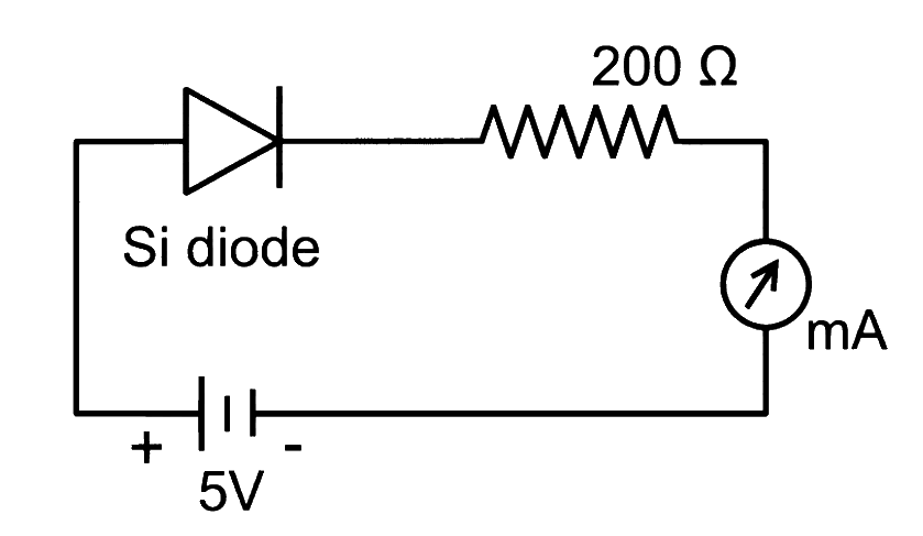
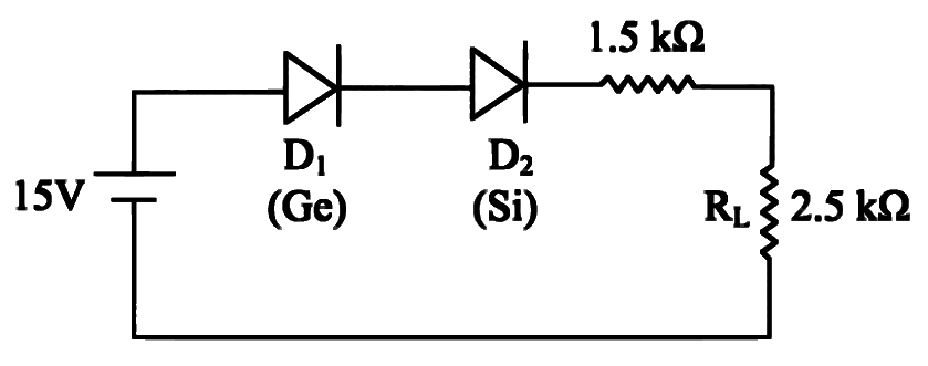
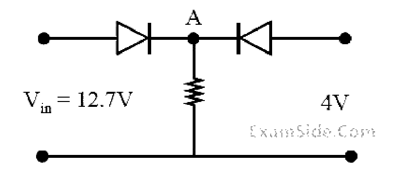
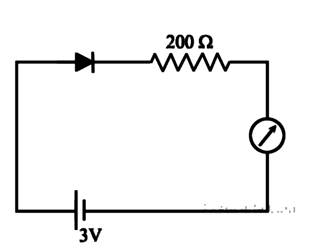
In the following electrical circuit, the reading in the milliammeter is
(Take knee voltage of silicon diode = 0.7 = 0.7 = 0.7
(a) 25.5 25.5 25.5 (b) 21.5 21.5 21.5 (c) 18.5 18.5 18.5 (d) 15.8 15.8 15.8 Show answer and solution
Answer: (b)
Loading the solution…
Report a mistake Q15 MHT CET 2026 · 17 APR · SHIFT 1 Medium ☆
P-N Junction Diode
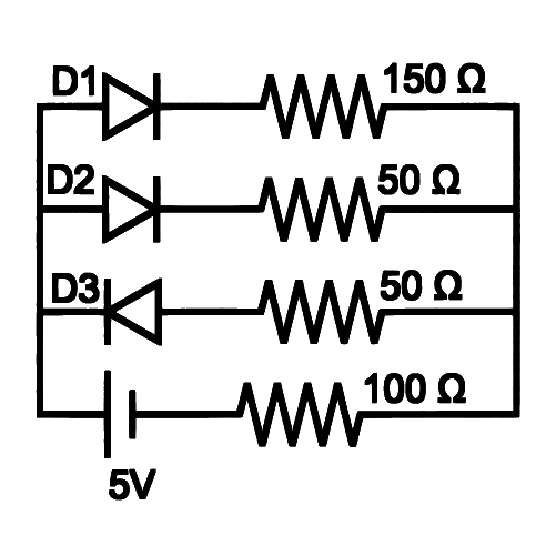
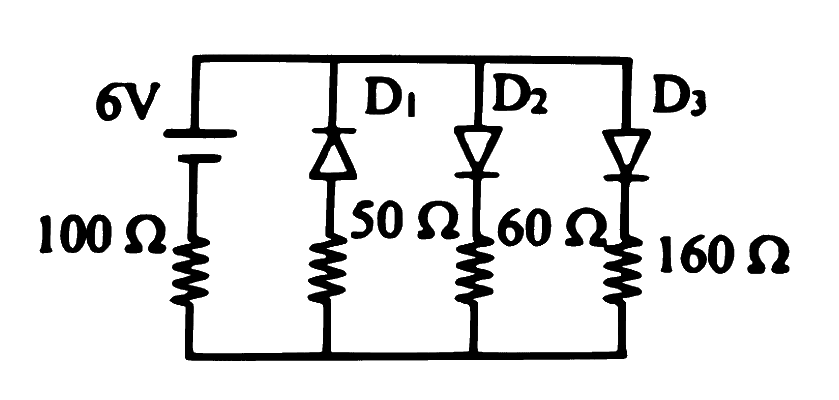
In the circuit shown in figure all the three diodes D1, D2, D3 have forward resistance 50 Ω 50\ \Omega 50 Ω 100 Ω 100\ \Omega 100 Ω
(a) 60 60 60 (b) 30 30 30 (c) 20 20 20 (d) 10 10 10 Show answer and solution
Answer: (b)
Loading the solution…
Report a mistake Q16 MHT CET 2026 · 15 APR · SHIFT 2 Medium ☆
P-N Junction Diode
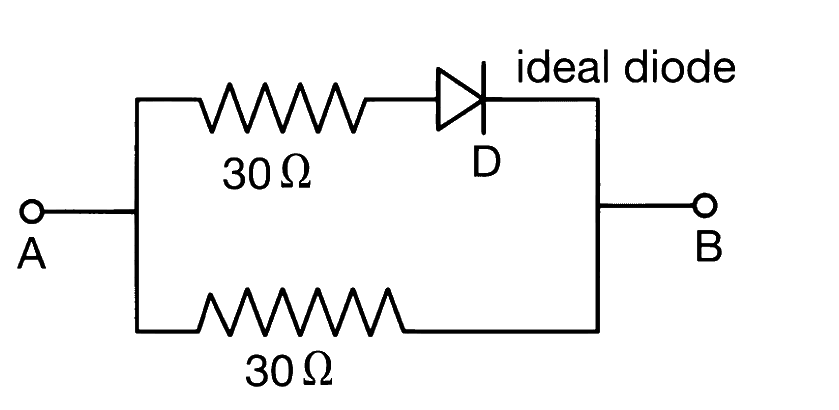
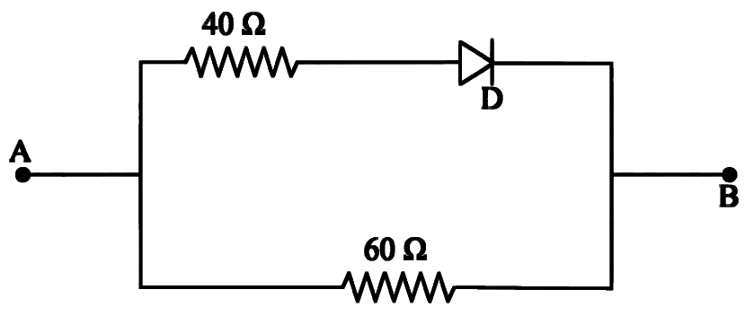
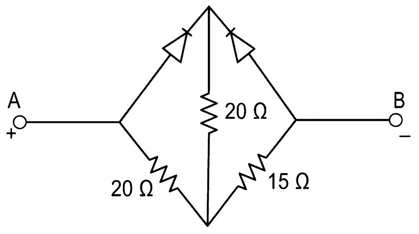
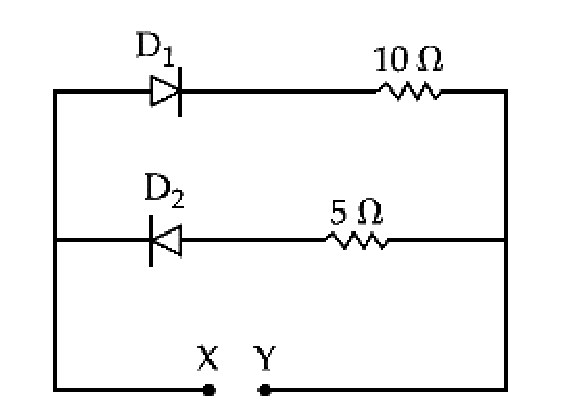
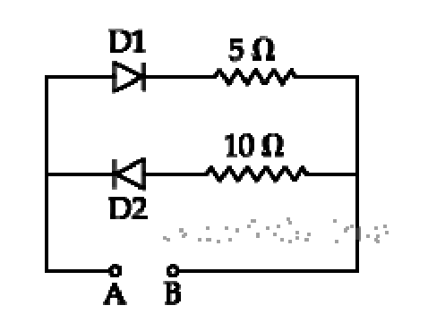
In the diagram shown, the resistance between points A and B is 'R 1 R_1 R 1 R 2 R_2 R 2 R 1 / R 2 R_1/R_2 R 1 / R 2
(a) 2 2 2 (b) 1 1 1 (c) 1 2 \frac{1}{2} 2 1 (d) 1 4 \frac{1}{4} 4 1 Show answer and solution
Answer: (c)
Loading the solution…
Report a mistake Q17 NEET 2026 Medium ☆
P-N Junction Diode
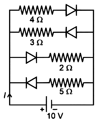
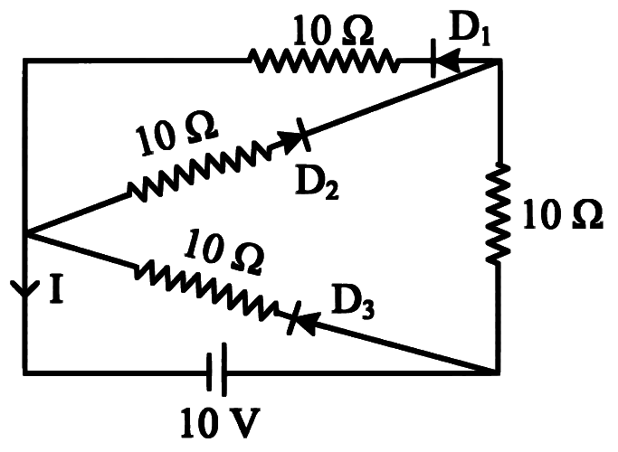
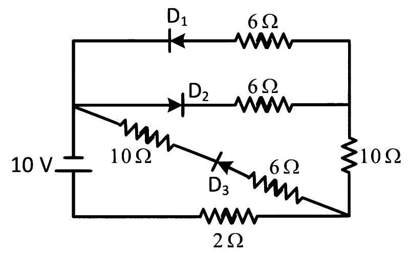
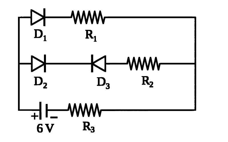
The current / in the circuit shown below is: (All diodes are ideal and identical)
(a) 5 3 A \frac{5}{3}\text{ A} 3 5 A (b) 5 9 A \frac{5}{9}\text{ A} 9 5 A (c) 1 3 A \frac{1}{3}\text{ A} 3 1 A (d) 15 2 A \frac{15}{2}\text{ A} 2 15 A Show answer and solution
Answer: (d)
Loading the solution…
Report a mistake Q18 JEE Main 2026 · 28 JAN · SHIFT 1 Medium ☆
P-N Junction Diode
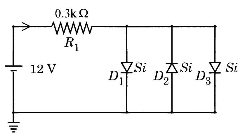
Assuming in forward bias condition there is a voltage drop of 0.7 V across a silicon diode, the current through diode D 1 D_1 D 1 ______ mA.
(Assume all diodes in the given circuit are identical)
(a) 17.6 (b) 18.8 (c) 20.15 (d) 11.7 Show answer and solution
Answer: (b)
Loading the solution…
Report a mistake Q19 NEET 2026 Medium ☆
P-N Junction Diode
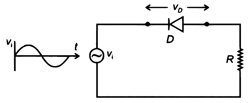
In the circuit shown below, the voltage appearing across the diode D will be of the form:
Show answer and solution
Answer: (d)
Loading the solution…
Report a mistake Q20 JEE Main 2026 · 21 JAN · SHIFT 2 Medium ☆
P-N Junction Diode
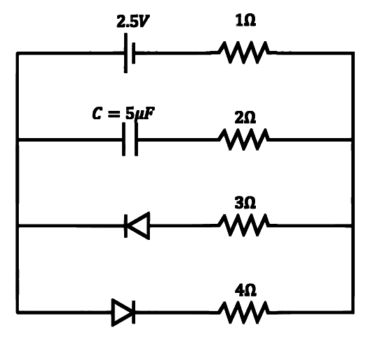
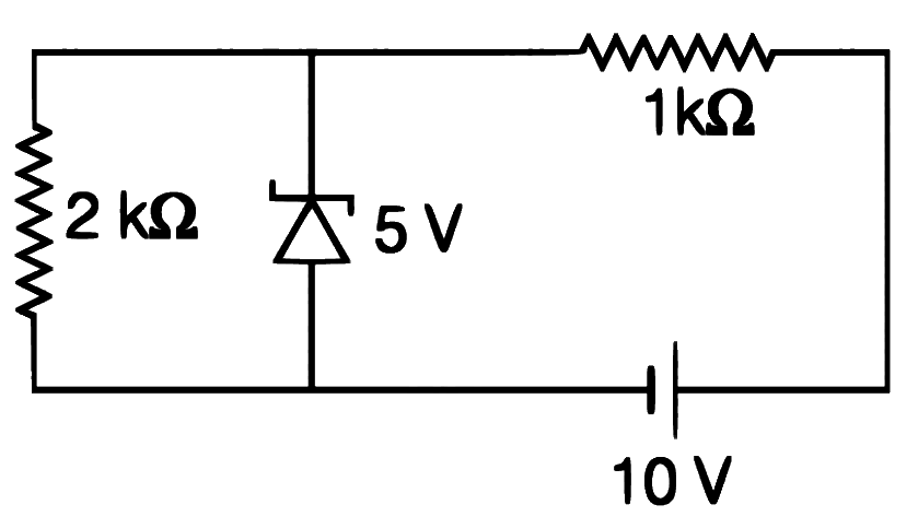
The charge stored by the capacitor C in the given circuit in the steady state is __________ µC.
Show answer and solution
Answer: (c)
Loading the solution…
Report a mistake Q21 JEE Main 2026 · 4 APR · SHIFT 1 Difficult ☆
P-N Junction Diode
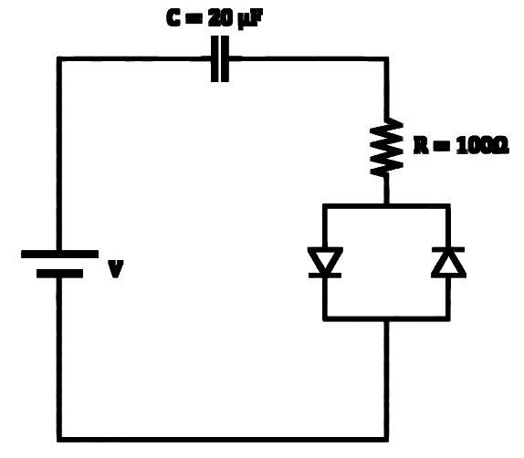
Consider a circuit consisting of a capacitor ( 20 μ F ) (20\,\mu\text{F}) ( 20 μ F ) ( 100 Ω ) (100\,\Omega) ( 100 Ω ) 10 Ω 10\,\Omega 10 Ω α × 1 0 − 3 s \alpha \times 10^{-3}\text{ s} α × 1 0 − 3 s α \alpha α ______
Show answer and solution
Answer: (a)
Loading the solution…
Report a mistake Q22 JEE Main 2026 · 2 APR · SHIFT 1 Difficult ☆
P-N Junction Diode
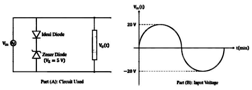
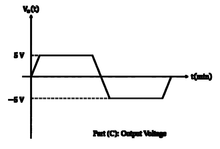
For the given circuit (shown in part (A)) the time dependent input voltage v i n ( t ) v_{in}(t) v in ( t ) v o ( t ) v_{o}(t) v o ( t )
Show answer and solution
Answer: (b)
Loading the solution…
Report a mistake Q23 MHT CET 2025 · 19 APR · SHIFT 1 Easy ☆
P-N Junction Diode
In the depletion layer of reverse biased p-n junction, the
(a) electric field is very small. (b) potential is maximum. (c) electric field is maximum. (d) potential is zero. Show answer and solution
Answer: (c)
Loading the solution…
Report a mistake Q24 MHT CET 2025 · 5 MAY · SHIFT 2 Easy ☆
P-N Junction Diode
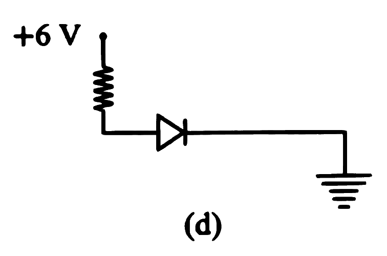
Which of the following figure represents forward bias diode?
Show answer and solution
Answer: (a)
Loading the solution…
Report a mistake Q25 MHT CET 2025 · 26 APR · SHIFT 2 Easy ☆
P-N Junction Diode
If p-n junction diode is forward biased, then
(a) electric conduction is not possible. (b) width of depletion layer decreases. (c) width of depletion layer increases. (d) barrier voltage increases. Show answer and solution
Answer: (b)
Loading the solution…
Report a mistake Q26 MHT CET 2025 · 26 APR · SHIFT 1 Easy ☆
P-N Junction Diode
Applying forward bias to p-n junction, the potential barrier
(a) increases. (b) decreases. (c) remains unchanged. (d) becomes zero. Show answer and solution
Answer: (b)
Loading the solution…
Report a mistake Q27 MHT CET 2025 · 25 APR · SHIFT 1 Easy ☆
P-N Junction Diode
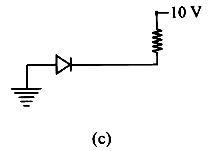
In which of the following figures, the p.n. junction diode is reverse biased?
Show answer and solution
Answer: (c)
Loading the solution…
Report a mistake Q28 JEE Main 2025 · 22 JAN · SHIFT 1 Easy ☆
P-N Junction Diode
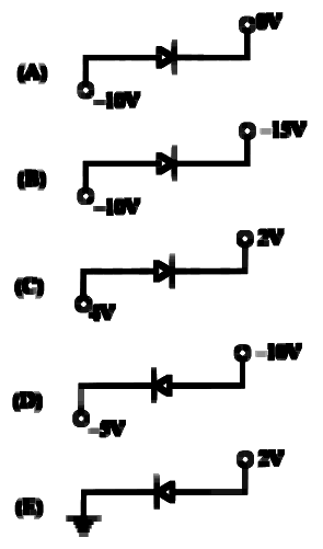
Which of the following circuits represents a forward biased diode?
Choose the correct answer from the options given below:
(a) (C) and (E) only (b) (A) and (D) only (c) (B), (D) and (E) only (d) (B), (C) and (E) only Show answer and solution
Answer: (d)
Loading the solution…
Report a mistake Q29 MHT CET 2025 · 20 APR · SHIFT 1 Easy ☆
P-N Junction Diode
For an ideal diode, in forward and reverse biased condition the resistance is respectively
(a) infinite, zero. (b) infinite, infinite. (c) zero, zero. (d) zero, infinite. Show answer and solution
Answer: (d)
Loading the solution…
Report a mistake Q30 MHT CET 2025 · 19 APR · SHIFT 2 Medium ☆
P-N Junction Diode
In unbiased p-n junction diode
(a) the potential is same everywhere. (b) there is an electric field at the junction directed from the p -type side to the n -type side. (c) there is an electric field at the junction directed from the n n n p p p (d) the p-type side is at higher potential than the n-type side. Show answer and solution
Answer: (c)
Loading the solution…
Report a mistake Q31 MHT CET 2025 · 21 APR · SHIFT 2 Medium ☆
P-N Junction Diode
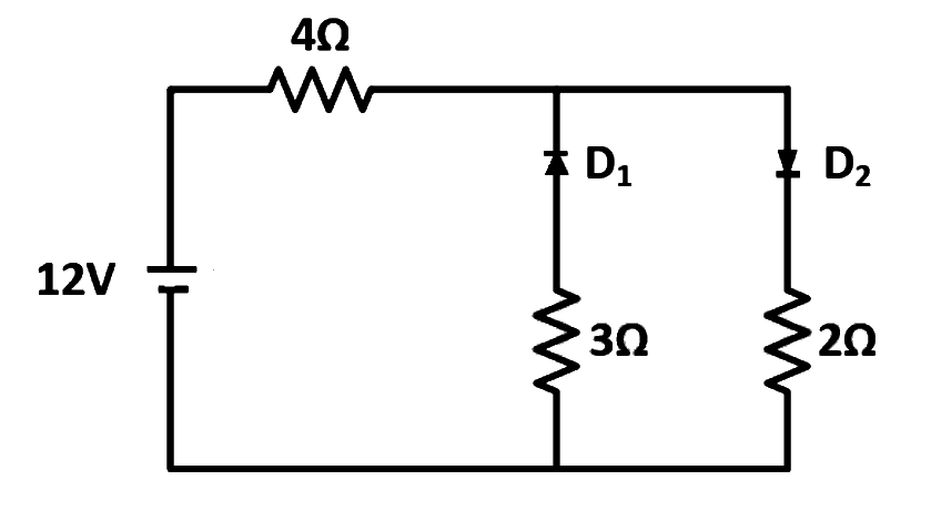
If the internal resistance of cell is negligible then current flowing through the circuit is
(a) 0.04 A 0.04\text{ A} 0.04 A (b) 0.06 A (c) 0.08 A (d) 0.10 A Show answer and solution
Answer: (d)
Loading the solution…
Report a mistake Q32 MHT CET 2025 · 20 APR · SHIFT 2 Medium ☆
P-N Junction Diode
In the following circuit shown in figure, three diodes are connected each with forward resistance 40 Ω 40\ \Omega 40 Ω 100 Ω 100\ \Omega 100 Ω
(a) 18 mA (b) 36 mA (c) 9 mA (d) 27 mA Show answer and solution
Answer: (b)
Loading the solution…
Report a mistake Q33 JEE Main 2025 · 23 JAN · SHIFT 2 Medium ☆
P-N Junction Diode
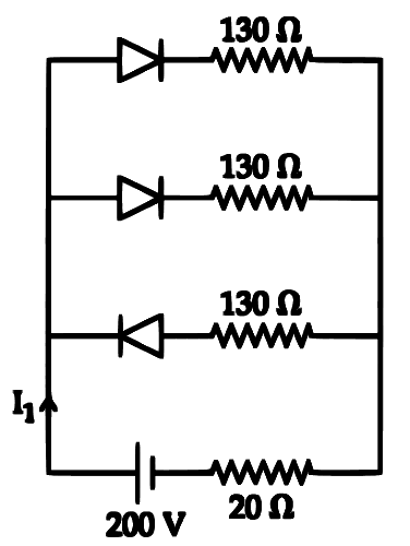
What is the current through the battery in the circuit shown below?
(a) 1.5 A (b) 0.25 A (c) 1.0 A (d) 0.5 A Show answer and solution
Answer: (d)
Loading the solution…
Report a mistake Q34 JEE Main 2025 · 23 JAN · SHIFT 1 Medium ☆
P-N Junction Diode
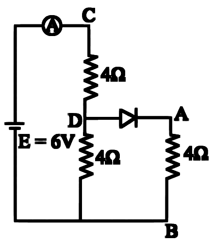
Refer to the circuit diagram given in the figure. which of the following observations are correct? A. Total resistance of circuit is 6 Ω 6\ \Omega 6 Ω
B. Current in Ammeter is 1 A
C. Potential across A B AB A B
D. Potential across CD is 4 Volts
E. Total resistance of the circuit is 8 Ω 8\ \Omega 8 Ω
Choose the correct answer from the options given below:
(a) B, C and E Only (b) A, C and D Only (c) A, B and C Only (d) A, B and D Only Show answer and solution
Answer: (d)
Loading the solution…
Report a mistake Q35 JEE Main 2025 · 8 APR · SHIFT 2 Medium ☆
P-N Junction Diode
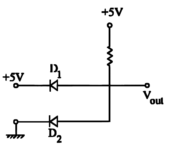
The output voltage in the following circuit is (Consider ideal diode case)
(a) 0 V (b) +5 V (c) −5 V (d) 10 V Show answer and solution
Answer: (a)
Loading the solution…
Report a mistake Q36 MHT CET 2024 · 4 MAY · SHIFT 2 Easy ☆
P-N Junction Diode
The depletion layer in p-n junction region is caused by
(a) drift of electrons. (b) migration of impurity ions. (c) diffusion of charge carries. (d) drift of holes. Show answer and solution
Answer: (c)
Loading the solution…
Report a mistake Q37 MHT CET 2024 · 2 MAY · SHIFT 2 Easy ☆
P-N Junction Diode
The potential barrier in p-n junction diode is due to
(a) depletion of positive charges near the junction. (b) accumulation of positive charges near the junction. (c) depletion of negative charges near the junction. (d) accumulation of positive and negative charges near the junction. Show answer and solution
Answer: (d)
Loading the solution…
Report a mistake Q38 MHT CET 2024 · 11 MAY · SHIFT 1 Easy ☆
P-N Junction Diode
A p-n junction diode cannot be used
(a) as a rectifier. (b) for converting light energy to electrical energy. (c) for getting light radiation. (d) for increasing the amplitude of an a.c. signal. Show answer and solution
Answer: (d)
Loading the solution…
Report a mistake Q39 MHT CET 2024 · 4 MAY · SHIFT 1 Easy ☆
P-N Junction Diode
A semiconductor device X is connected in series with a battery and a resistor. The current of 10 mA is found to pass through the circuit. If the terminals of X are connected in reverse manner, the current drops to almost zero. X may be
(a) a zener diode (b) a p-n junction diode (c) an intrinsic semiconductor (d) an extrinsic semiconductor Show answer and solution
Answer: (b)
Loading the solution…
Report a mistake Q40 JEE Main 2024 · 27 JAN · SHIFT 1 Easy ☆
P-N Junction Diode
Which of the following circuits is reverse - biased?
Show answer and solution
Answer: (d)
Loading the solution…
Report a mistake Q41 MHT CET 2024 · 11 MAY · SHIFT 2 Easy ☆
P-N Junction Diode
Assuming that junction diode is ideal, the current in arrangement shown in figure
(a) 2 mA (b) 20 mA (c) 30 mA (d) 10 mA Show answer and solution
Answer: (b)
Loading the solution…
Report a mistake Q42 MHT CET 2024 · 16 MAY · SHIFT 1 Medium ☆
P-N Junction Diode
If the p - n p\text{-}n p - n
(a) n-type side has lower potential than p-type side. (b) n-type side has same potential as p-type side. (c) An electric field is established at the junction such that n side is at positive voltage relative to p - side. (d) The potential across the junction is such that p -side is at positive voltage relative to n-side Show answer and solution
Answer: (c)
Loading the solution…
Report a mistake Q43 JEE Main 2024 · 4 APR · SHIFT 2 Medium ☆
P-N Junction Diode
Which of the diode circuits shows correct biasing used for the measurement of dynamic resistance of p-n junction diode:
Show answer and solution
Answer: (d)
Loading the solution…
Report a mistake Q44 MHT CET 2024 · 15 MAY · SHIFT 2 Medium ☆
P-N Junction Diode
What is the current in the following junction diode circuit?
(a) 1 0 − 1 A 10^{-1}\text{ A} 1 0 − 1 A (b) zero (c) 1 0 − 2 A 10^{-2}\text{ A} 1 0 − 2 A (d) 5 × 1 0 − 3 A 5 \times 10^{-3}\text{ A} 5 × 1 0 − 3 A Show answer and solution
Answer: (b)
Loading the solution…
Report a mistake Q45 MHT CET 2024 · 10 MAY · SHIFT 1 Medium ☆
P-N Junction Diode
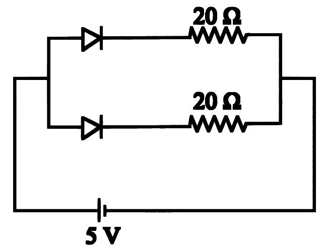
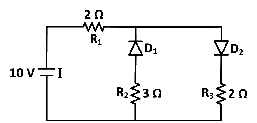
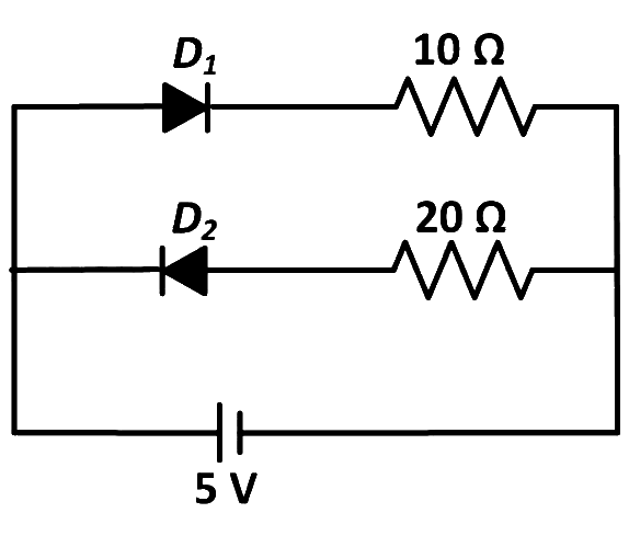
Two ideal diodes are connected to a battery as shown in the circuit. The current supplied by the battery is
(a) zero (b) 0.25 A (c) 0.50 A (d) 0.75 A Show answer and solution
Answer: (b)
Loading the solution…
Report a mistake Q46 MHT CET 2024 · 9 MAY · SHIFT 1 Medium ☆
P-N Junction Diode
For the diagram shown, the resistance between points A and B when the ideal diode ' D D D R 1 R_1 R 1 R 2 R_2 R 2 R 1 R 2 \frac{R_1}{R_2} R 2 R 1
(a) 2 3 \frac{2}{3} 3 2 (b) 2 5 \frac{2}{5} 5 2 (c) 3 2 \frac{3}{2} 2 3 (d) 5 2 \frac{5}{2} 2 5 Show answer and solution
Answer: (b)
Loading the solution…
Report a mistake Q47 MHT CET 2024 · 3 MAY · SHIFT 1 Medium ☆
P-N Junction Diode
Find the magnitude of current in the given circuit.
(a) zero ampere (b) 1 ampere (c) 0.1 ampere (d) 0.2 ampere Show answer and solution
Answer: (a)
Loading the solution…
Report a mistake Q48 JEE Main 2024 · 4 APR · SHIFT 1 Medium ☆
P-N Junction Diode
The value of net resistance of the network as shown in the given figure is:
(a) ( 30 / 11 ) Ω (30/11)\ \Omega ( 30/11 ) Ω (b) 6 Ω 6\ \Omega 6 Ω (c) ( 5 / 2 ) Ω (5/2)\ \Omega ( 5/2 ) Ω (d) ( 15 / 4 ) Ω (15/4)\ \Omega ( 15/4 ) Ω Show answer and solution
Answer: (b)
Loading the solution…
Report a mistake Q49 JEE Main 2024 · 30 JAN · SHIFT 2 Medium ☆
P-N Junction Diode
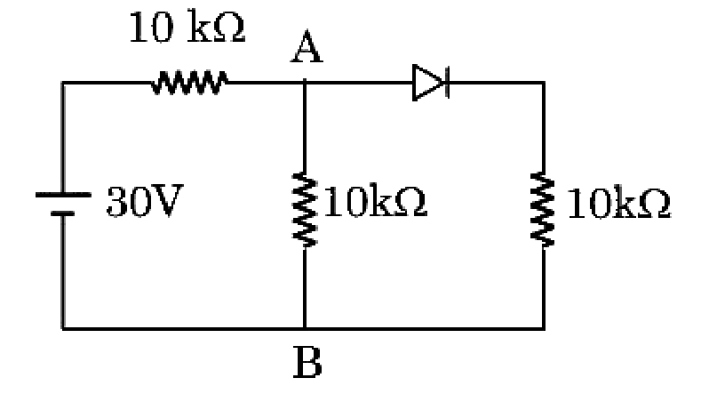
In the given circuit, the voltage across load resistance (RL {}_L L
(a) 8.75 V (b) 9.00 V (c) 8.50 V (d) 14.00 V Show answer and solution
Answer: (a)
Loading the solution…
Report a mistake Q50 MHT CET 2023 · 13 MAY · SHIFT 1 Easy ☆
P-N Junction Diode
On increasing the reverse bias to a large value in a P-N junction diode, current
(a) increase slowly. (b) remains fixed. (c) suddenly increases. (d) decreases slowly. Show answer and solution
Answer: (c)
Loading the solution…
Report a mistake Q51 MHT CET 2023 · 12 MAY · SHIFT 2 Easy ☆
P-N Junction Diode
In which figure, the junction diode is forward biased?
Show answer and solution
Answer: (b)
Loading the solution…
Report a mistake Q52 MHT CET 2023 · 12 MAY · SHIFT 1 Easy ☆
P-N Junction Diode
When forward bias is applied to a p-n junction, then what happens to the potential barrier ( V B ) (V_B) ( V B ) ( X ) (X) ( X )
(a) V B V_B V B X X X (b) V B V_B V B X X X (c) V B V_B V B X X X (d) V B V_B V B X X X Show answer and solution
Answer: (d)
Loading the solution…
Report a mistake Q53 MHT CET 2023 · 11 MAY · SHIFT 2 Easy ☆
P-N Junction Diode
If p - n p\text{-}n p - n
(a) width of depletion layer increases (b) electric conduction is not possible at all (c) barrier voltage increases (d) width of depletion layer decreases Show answer and solution
Answer: (d)
Loading the solution…
Report a mistake Q54 MHT CET 2023 · 9 MAY · SHIFT 2 Easy ☆
P-N Junction Diode
In the reverse biasing of a p-n junction diode:
(a) the width of the depletion layer decreases. (b) the width of the depletion layer increases. (c) the number of minority charge carriers increase. (d) the number of majority charge carriers increase. Show answer and solution
Answer: (b)
Loading the solution…
Report a mistake Q55 JEE Main 2023 · 25 JAN · SHIFT 2 Medium ☆
P-N Junction Diode
Statement I: When a Si sample is doped with Boron, it becomes P type and when doped by Arsenic it becomes N-type semi conductor such that P-type has excess holes and N-type has excess electrons.
Statement II: When such P-type and N-type semi-conductors, are fused to make a junction, a current will automatically flow which can be detected with an externally connected ameter. In the light of above statements, choose the most appropriate answer from the options given below
(a) Statement I is incorrect but statement II is correct (b) Both Statement I and statement II are correct (c) Statement I is correct but statement II is incorrect (d) Both Statement I and Statement II are incorrect Show answer and solution
Answer: (c)
Loading the solution…
Report a mistake Q56 JEE Main 2023 · 6 APR · SHIFT 2 Medium ☆
P-N Junction Diode
Given below are two statements: one is labelled as Assertion A and the other is labelled as Reason R
Assertion A: Diffusion current in a p-n junction is greater than the drift current in magnitude if the junction is forward biased.
Reason R: Diffusion current in a p-n junction is from the n n n
In the light of the above statements, choose the most appropriate answer from the options given below
(a) Both A and R are correct but R is NOT the correct explanation of A (b) A is correct but R is not correct (c) A is not correct but R is correct (d) Both A and R are correct and R is the correct explanation of A Show answer and solution
Answer: (b)
Loading the solution…
Report a mistake Q57 MHT CET 2023 · 10 MAY · SHIFT 2 Medium ☆
P-N Junction Diode
For the diagram shown, the resistances between points A and B when ideal diode D is forward biased is 'R 1 R_1 R 1 R 2 R_2 R 2 R 1 : R 2 R_1 : R_2 R 1 : R 2
(a) 2: 1 (b) 1: 1 (c) 1: 2 (d) 1: 4 Show answer and solution
Answer: (c)
Loading the solution…
Report a mistake Q58 JEE Main 2023 · 15 APR · SHIFT 1 Medium ☆
P-N Junction Diode
In the given circuit, the current (I) through the battery will be
(a) 1A (b) 2.5 A 2.5\text{ A} 2.5 A (c) 2 A 2\text{ A} 2 A (d) 1.5 A 1.5\text{ A} 1.5 A Show answer and solution
Answer: (d)
Loading the solution…
Report a mistake Q59 JEE Main 2023 · 10 APR · SHIFT 2 Medium ☆
P-N Junction Diode
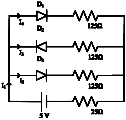
If each diode has a forward bias resistance of 25 Ω 25\ \Omega 25 Ω
Which of the following options is correct:
(a) I 3 I 4 = 1 \frac{I_3}{I_4} = 1 I 4 I 3 = 1 (b) I 1 I 2 = 2 \frac{I_1}{I_2} = 2 I 2 I 1 = 2 (c) I 2 I 3 = 1 \frac{I_2}{I_3} = 1 I 3 I 2 = 1 (d) I 1 I 2 = 1 \frac{I_1}{I_2} = 1 I 2 I 1 = 1 Show answer and solution
Answer: (b)
Loading the solution…
Report a mistake Q60 JEE Main 2022 · 29 JUL · SHIFT 1 Easy ☆
P-N Junction Diode
If the potential barrier across a p-n junction is 0.6 V 0.6\text{ V} 0.6 V 6 × 1 0 − 6 m 6 \times 10^{-6}\text{ m} 6 × 1 0 − 6 m × 1 0 5 N/C \times 10^{5}\text{ N/C} × 1 0 5 N/C
Numerical answer type. Work it out, then open the answer.
Show answer and solution
Answer: 1
Loading the solution…
Report a mistake Q61 JEE Main 2022 · 28 JUN · SHIFT 1 Easy ☆
P-N Junction Diode
For using a multimeter to identify diode from electrical components, choose the correct statement out of the following about the diode:
(a) It is two terminal device which conducts current in both directions. (b) It is two terminal device which conducts current in one direction only. (c) It does not conduct current gives an initial deflection which decays to zero. (d) It is three terminal device which conducts current in one direction only between central terminal and either of the remaining two terminals Show answer and solution
Answer: (b)
Loading the solution…
Report a mistake Q62 JEE Main 2022 · 26 JUN · SHIFT 1 Medium ☆
P-N Junction Diode
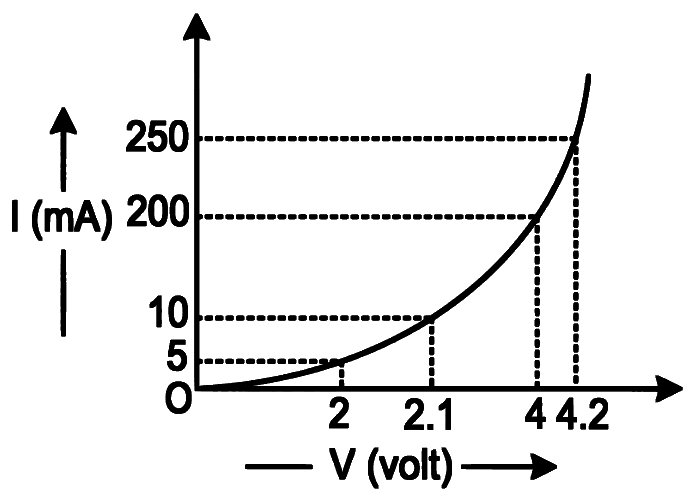
The I-V characteristics of a p-n junction diode in forward bias is shown in the figure. The ratio of dynamic resistance, corresponding to forward bias voltage of 2 V and 4 V respectively, is:
(a) 1: 2 (b) 5: 1 (c) 1: 40 (d) 20: 1 Show answer and solution
Answer: (b)
Loading the solution…
Report a mistake Q63 MHT CET 2022 · 11 AUG · SHIFT 2 Medium ☆
P-N Junction Diode
The given circuit has two ideal diodes D 1 D_1 D 1 D 2 D_2 D 2 R 1 R_1 R 1
(a) 7 A (b) 3.3 A (c) 2 A (d) 2.5 A Show answer and solution
Answer: (c)
Loading the solution…
Report a mistake Q64 NEET 2022 · PHASE 1 Medium ☆
P-N Junction Diode
In the given circuits (a), (b) and (c), the potential drop across the two p-n junctions are equal in
(a) Circuit (a) only (b) Circuit (b) only (c) Circuit (c) only (d) Both circuits (a) and (c) Show answer and solution
Answer: (d)
Loading the solution…
Report a mistake Q65 JEE Main 2022 · 25 JUL · SHIFT 2 Medium ☆
P-N Junction Diode
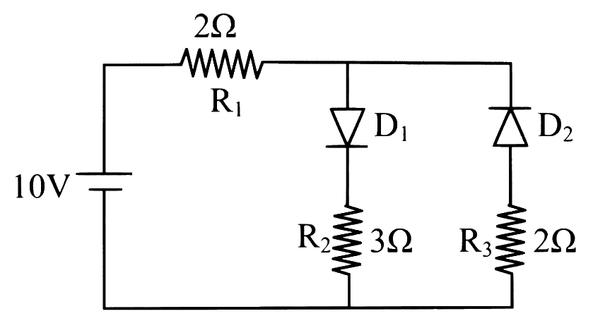
Two ideal diodes are connected in the network as shown in figure. The equivalent resistance between A and B is __________ Ω \Omega Ω
Numerical answer type. Work it out, then open the answer.
Show answer and solution
Answer: 25
Loading the solution…
Report a mistake Q66 JEE Main 2022 · 27 JUN · SHIFT 2 Medium ☆
P-N Junction Diode
The cut-off voltage of the diodes (shown in figure) in forward bias is 0.6 V. The current through the resistor of 40 Ω \Omega Ω
Numerical answer type. Work it out, then open the answer.
Show answer and solution
Answer: 4
Loading the solution…
Report a mistake Q67 JEE Main 2022 · 26 JUN · SHIFT 1 Medium ☆
P-N Junction Diode
As per the given circuit, the value of current through the battery will be ____________ A.
Numerical answer type. Work it out, then open the answer.
Show answer and solution
Answer: 1
Loading the solution…
Report a mistake Q68 JEE Main 2022 · 29 JUN · SHIFT 2 Difficult ☆
P-N Junction Diode
A potential barrier of 0.4 V exists across a p-n junction. An electron enters the junction from the n- side with a speed of 6.0 × \times × − 1 {}^{-1} − 1 x 3 × 1 0 5 \frac{x}{3} \times 10^{5} 3 x × 1 0 5 − 1 {}^{-1} − 1
(Given mass of electron = 9 × \times × − - − × \times × − - −
Numerical answer type. Work it out, then open the answer.
Show answer and solution
Answer: 14
Loading the solution…
Report a mistake Q69 JEE Main 2022 · 28 JUN · SHIFT 2 Difficult ☆
P-N Junction Diode
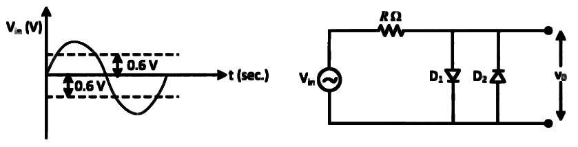
In the given circuit the input voltage Vin is shown in figure. The cut-in voltage of p-n junction diode (D1 or D2) is 0.6 V. Which of the following output voltage (V0) waveform across the diode is correct?
Show answer and solution
Answer: (d)
Loading the solution…
Report a mistake Q70 JEE Main 2021 · 20 JUL · SHIFT 2 Medium ☆
P-N Junction Diode
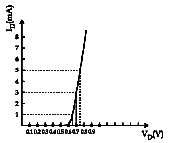
For the forward biased diode characteristics shown in the figure, the dynamic resistance at ID = 3 mA will be __________ Ω \Omega Ω
Numerical answer type. Work it out, then open the answer.
Show answer and solution
Answer: 25
Loading the solution…
Report a mistake Q71 MHT CET 2021 · 24 SEP · SHIFT 1 Medium ☆
P-N Junction Diode
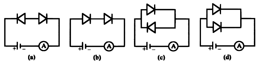
Two identical ideal diodes are connected to an ammeter and a d.c source (1 volt) as shown. In which one of the following circuits, ammeter will not show any deflection?
Show answer and solution
Answer: (b)
Loading the solution…
Report a mistake Q72 MHT CET 2021 · 23 SEP · SHIFT 1 Medium ☆
P-N Junction Diode
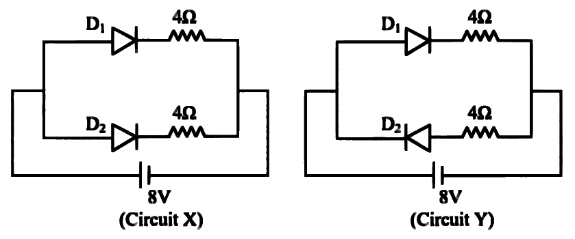
What are the values of the currents flowing in each of the following diode circuits X \text{X} X Y \text{Y} Y
(a) 1 A, 2 A (b) 2 A, 1 A (c) 4 A, 2 A (d) 2 A, 4 A Show answer and solution
Answer: (c)
Loading the solution…
Report a mistake Q73 MHT CET 2021 · 21 SEP · SHIFT 2 Medium ☆
P-N Junction Diode
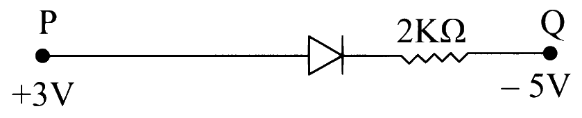
In an ideal junction diode, the current flowing through PQ is
(a) 2 × \times × − 3 {}^{-3} − 3 (b) 2 × \times × − 2 {}^{-2} − 2 (c) 4 × \times × − 3 {}^{-3} − 3 (d) 10− 3 {}^{-3} − 3 Show answer and solution
Answer: (c)
Loading the solution…
Report a mistake Q74 MHT CET 2021 · 21 SEP · SHIFT 1 Medium ☆
P-N Junction Diode
The current in the following circuit is
(a) 10 A (b) zero (c) 0.025 A (d) 10− 2 {}^{-2} − 2 Show answer and solution
Answer: (d)
Loading the solution…
Report a mistake Q75 JEE Main 2021 · 1 SEP · SHIFT 2 Medium ☆
P-N Junction Diode
In the given figure, each diode has a forward bias resistance of 30Ω \Omega Ω
(a) 3.75 A (b) 2.35 A (c) 2 A (d) 2.73 A Show answer and solution
Answer: (c)
Loading the solution…
Report a mistake Q76 JEE Main 2021 · 25 FEB · SHIFT 1 Medium ☆
P-N Junction Diode
A 5V battery is connected across the points X and Y. Assume D1 and D2 to be normal silicon diodes. Find the current supplied by the battery if the +ve terminal of the battery is connected to point X.
(a) ∼ \sim ∼ (b) ∼ \sim ∼ (c) ∼ \sim ∼ (d) ∼ \sim ∼ Show answer and solution
Answer: (c)
Loading the solution…
Report a mistake Q77 JEE Main 2021 · 26 FEB · SHIFT 1 Medium ☆
P-N Junction Diode
The circuit contains two diodes each with a forward resistance of 50Ω \Omega Ω Ω \Omega Ω
Numerical answer type. Work it out, then open the answer.
Show answer and solution
Answer: 20
Loading the solution…
Report a mistake Q78 JEE Main 2021 · 24 FEB · SHIFT 1 Medium ☆
P-N Junction Diode
In connection with the circuit drawn below, the value of current flowing through 2 kΩ \Omega Ω × \times × − - −
Numerical answer type. Work it out, then open the answer.
Show answer and solution
Answer: 25
Loading the solution…
Report a mistake Q79 NEET 2020 · PHASE 1 Easy ☆
P-N Junction Diode
The increase in the width of the depletion region in a p-n junction diode is due to:
(a) reverse bias only (b) both forward bias and reverse bias (c) increase in forward current (d) forward bias only Show answer and solution
Answer: (a)
Loading the solution…
Report a mistake Q80 NEET 2020 · PHASE 2 Easy ☆
P-N Junction Diode
Out of the following which one is a forward biased diode?
Show answer and solution
Answer: (a)
Loading the solution…
Report a mistake Q81 JEE Main 2020 · 3 SEP · SHIFT 1 Easy ☆
P-N Junction Diode
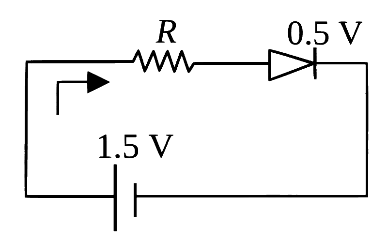
When a diode is forward biased, it has a voltage drop of 0.5 V. The safe limit of current through the diode is 10 mA. If a battery of emf 1.5 V is used in the circuit, the value of minimum resistance to be connected in series with the diode so that the current does not exceed the safe limit is
(a) 50 Ω \Omega Ω (b) 200 Ω \Omega Ω (c) 300 Ω \Omega Ω (d) 100 Ω \Omega Ω Show answer and solution
Answer: (d)
Loading the solution…
Report a mistake Q82 JEE Main 2020 · 3 SEP · SHIFT 2 Medium ☆
P-N Junction Diode
Which of the following will NOT be observed when a multimeter (operating in resistance measuring mode) probes connected across a component, are just reversed?
(a) Multimeter shows NO deflection in both cases i.e. before and after reversing the probes if the chosen component is metal wire. (b) Multimeter shows a deflection, accompanied by a splash of light out of connected component in one direction and NO deflection on reversing the probes if the chosen component is LED. (c) Multimeter shows an equal deflection in both cases i.e. before and after reversing the probes if the chosen component is resistor. (d) Multimeter shows NO deflection in both cases i.e. before and after reversing the probes if the chosen component is capacitor. Show answer and solution
Answer: (d)
Loading the solution…
Report a mistake Q83 JEE Main 2020 · 9 JAN · SHIFT 2 Medium ☆
P-N Junction Diode
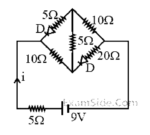
The current i in the network is:
(a) 0.6 A (b) 0.3 A (c) 0 A (d) 0.2 A Show answer and solution
Answer: (b)
Loading the solution…
Report a mistake Q84 JEE Main 2020 · 7 JAN · SHIFT 2 Medium ☆
P-N Junction Diode
In the figure, potential difference between A and B is:
(a) 10 V (b) 5 V (c) zero (d) 15 V Show answer and solution
Answer: (a)
Loading the solution…
Report a mistake Q85 JEE Main 2020 · 9 JAN · SHIFT 2 Difficult ☆
P-N Junction Diode
Two identical capacitors A and B, charged to the same potential 5V are connected in two different circuits as shown below at time t = 0. If the charge on capacitors A and B at time t = CR is QA and QB respectively, then (Here e is the base of natural logarithm)
(a) QA = C V e \frac{CV}{e} e C V V C 2 \frac{VC}{2} 2 V C (b) QA = C V 2 \frac{CV}{2} 2 C V V C e \frac{VC}{e} e V C (c) QA = VC, QB = V C e \frac{VC}{e} e V C (d) QA = VC, QB = CV Show answer and solution
Answer: (c)
Loading the solution…
Report a mistake Q86 JEE Main 2020 · 9 JAN · SHIFT 1 Difficult ☆
P-N Junction Diode
Both the diodes used in the circuit shown are assumed to be ideal and have negligible resistance when these are forward biased. Built in potential in each diode is 0.7 V. For the input voltages shown in the figure, the voltage (in Volts) at point A is __________.
Numerical answer type. Work it out, then open the answer.
Show answer and solution
Answer: 12
Loading the solution…
Report a mistake Q87 MHT CET 2019 · 2 MAY · SHIFT 2 Easy ☆
P-N Junction Diode
In case of p p p
(a) decreased with heavy doping (b) increased by reverse biasing (c) decreased with light doping (d) increased by forward biasing Show answer and solution
Answer: (b)
Loading the solution…
Report a mistake Q88 MHT CET 2019 · 2 MAY · SHIFT 1 Easy ☆
P-N Junction Diode
Assuming that the junction diode is ideal, the current in the arrangement shown in figure is
(a) 30 mA (b) 40 mA (c) 20 mA (d) 10 mA Show answer and solution
Answer: (c)
Loading the solution…
Report a mistake Q89 JEE Main 2019 · 11 JAN · SHIFT 2 Medium ☆
P-N Junction Diode
The circuit shown below contains two ideal diodes, each with a forward resistance of 50 Ω \Omega Ω Ω \Omega Ω
(a) 0.027 (b) 0.030 (c) 0.036 (d) 0.020 Show answer and solution
Answer: (d)
Loading the solution…
Report a mistake Q90 JEE Main 2019 · 9 JAN · SHIFT 2 Difficult ☆
P-N Junction Diode
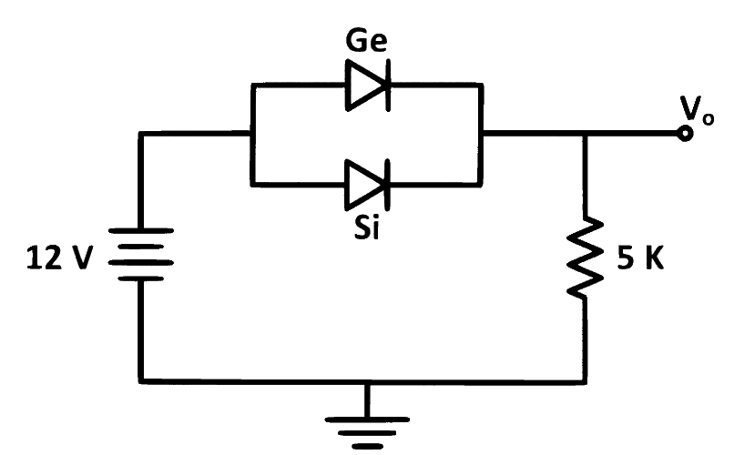
Ge and Si diodes start conducting at 0.3 V and 0.7 V respectively. In the following figure if Ge diode connection are reversed, the value of V0 changes by: (assume that the Ge diode has large breakdown voltage)
(a) 0.8 V (b) 0.6 V (c) 0.2 V (d) 0.4 V Show answer and solution
Answer: (d)
Loading the solution…
Report a mistake Q91 NEET 2018 Medium ☆
P-N Junction Diode
In a p-n junction diode, change in temperature due to heating
(a) affects only reverse resistance (b) affects only forward resistance (c) does not affect resistance of p-n junction (d) affects the overall V - I characteristics of p-n junction Show answer and solution
Answer: (d)
Loading the solution…
Report a mistake Q92 JEE Main 2018 Medium ☆
P-N Junction Diode
The reading of the ammeter for a silicon diode in the given circuit is:
(a) 13.5 mA (b) 0 (c) 15 mA (d) 11.5 mA Show answer and solution
Answer: (d)
Loading the solution…
Report a mistake Q93 NEET 2017 Easy ☆
P-N Junction Diode
Which one of the following represents forward bias diode?
Show answer and solution
Answer: (d)
Loading the solution…
Report a mistake Q94 JEE Main 2017 · 8 APR · SHIFT 1 Medium ☆
P-N Junction Diode
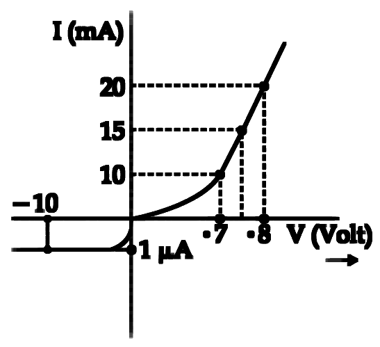
The V-I characteristic of a diode is shown in the figure. The ratio of forward to reverse bias resistance is:
(a) 10 (b) 10− {}^{-} − (c) 106 (d) 100 Show answer and solution
Answer: (b)
Loading the solution…
Report a mistake Q95 NEET 2016 · PHASE 1 Easy ☆
P-N Junction Diode
Consider the junction diode as ideal. The value of current flowing through AB is
(a) 10− {}^{-} − (b) 10− {}^{-} − (c) 0 A (d) 10− {}^{-} − Show answer and solution
Answer: (d)
Loading the solution…
Report a mistake Q96 NEET 2016 · PHASE 2 Medium ☆
P-N Junction Diode
The given circuit has two ideal diodes connected as shown in the figure. The current flowing through the resistance R1 will be
(a) 2.5 A (b) 10.0 A (c) 1.43 A (d) 3.13 A Show answer and solution
Answer: (a)
Loading the solution…
Report a mistake Q97 JEE Main 2015 · 10 APR · SHIFT 1 Easy ☆
P-N Junction Diode
In an unbiased n-p junction electrons diffuse from n - region to p - region because:
(a) holes in p - region attract them (b) electrons travel across the junction due to potential difference (c) electron concentration in n - region is more as compared to that in p - region (d) only electrons move from n to p region and not the vice - versa Show answer and solution
Answer: (c)
Loading the solution…
Report a mistake Q98 NEET 2015 · AIPMT Easy ☆
P-N Junction Diode
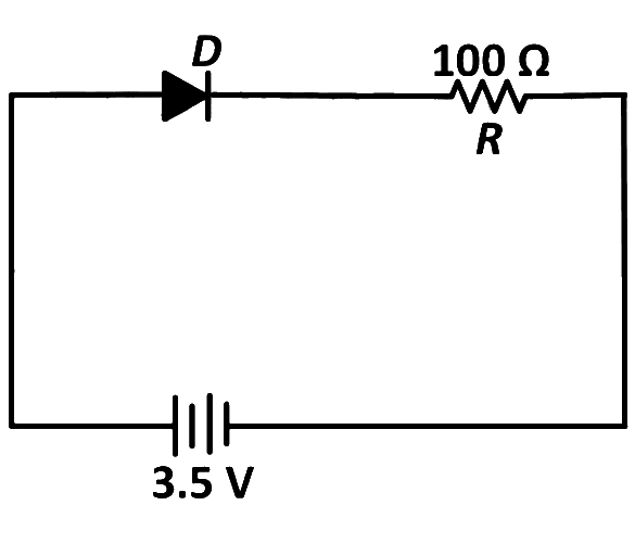
In the given figure, a diode D is connected to an external resistance R = 100 Ω \Omega Ω
(a) 20 mA (b) 35 mA (c) 30 mA (d) 40 mA Show answer and solution
Answer: (c)
Loading the solution…
Report a mistake Q99 JEE Main 2015 · 11 APR · SHIFT 1 Medium ☆
P-N Junction Diode
A 2V battery is connected across AB as shown in the figure. The value of the current supplied by the battery when in one case battery's positive terminal is connected to A and in other case when positive terminal of battery is connected to B will respectively be:
(a) 0.2 A and 0.1 A (b) 0.4 A and 0.2 A (c) 0.1 A and 0.2 A (d) 0.2 A and 0.4 A Show answer and solution
Answer: (b)
Loading the solution…
Report a mistake Q100 NEET 2015 · AIPMT · CANCELLED PAPER Medium ☆
P-N Junction Diode
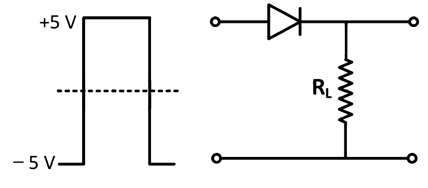
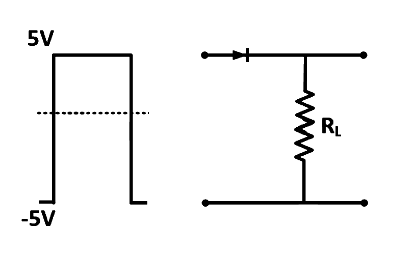
If in a p-n junction, a square input signal of 10 V is applied, as shown,
then the output across RL will be
Show answer and solution
Answer: (b)
Loading the solution…
Report a mistake Q101 JEE Main 2014 Easy ☆
P-N Junction Diode
The forward biased diode connection is:
Show answer and solution
Answer: (a)
Loading the solution…
Report a mistake Q102 NEET 2014 · AIPMT Medium ☆
P-N Junction Diode
The barrier potential of a p-n junction depends on
(1) type of semiconductor material
(2) amount of doping
(3) temperature
Which one of the following is correct?
(a) (1) and (2) only (b) (2) only (c) (2) and (3) only (d) (1), (2) and (3) Show answer and solution
Answer: (d)
Loading the solution…
Report a mistake Q103 JEE Main 2014 Difficult ☆
P-N Junction Diode
The current voltage relation of diode is given by I = ( e 1000 V / T − 1 ) mA , I = \left(e^{1000V/T} - 1\right)\text{ mA}, I = ( e 1000 V / T − 1 ) mA , V V V T T T ± 0.01 V \pm 0.01\,V ± 0.01 V 5 m A 5\,mA 5 m A 300 K , 300\,K, 300 K , m A mA m A
(a) 0.2 m A 0.2\,mA 0.2 m A (b) 0.02 m A 0.02\,mA 0.02 m A (c) 0.5 m A 0.5\,mA 0.5 m A (d) 0.05 m A 0.05\,mA 0.05 m A Show answer and solution
Answer: (a)
Loading the solution…
Report a mistake Q104 NEET 2013 Easy ☆
P-N Junction Diode
In an unbiased p-n junction, holes diffuse from the p-region to n-region because of
(a) The attraction of free electrons of n-region. (b) The higher hole concentration in p-region than that in n-region. (c) The higher concentration of electrons in the n-region than that in the p-region. (d) The potential difference across the p-n junction. Show answer and solution
Answer: (b)
Loading the solution…
Report a mistake Q105 JEE Main 2013 · 22 APR · SHIFT 1 Medium ☆
P-N Junction Diode
Figure shows a circuit in which three identical diodes are used. Each diode has forward resistance of 20Ω \Omega Ω R 1 = R 2 = R 3 = 50 Ω R_1 = R_2 = R_3 = 50\ \Omega R 1 = R 2 = R 3 = 50 Ω R 3 R_3 R 3
(a) 50 mA (b) 100 mA (c) 60 mA (d) 25 mA Show answer and solution
Answer: (a)
Loading the solution…
Report a mistake Q106 NEET 2012 · AIPMT · PRELIMS Medium ☆
P-N Junction Diode
Two ideal diodes are connected to a battery as shown in the circuit. The current supplied by the battery is
(a) 0.75 A (b) zero (c) 0.25 A (d) 0.5 A Show answer and solution
Answer: (d)
Loading the solution…
Report a mistake Q107 NEET 2011 · AIPMT · PRELIMS Easy ☆
P-N Junction Diode
In forward biasing of the p-n junction
(a) the positive terminal of the battery is connected to p-side and the depletion region becomes thick. (b) the positive terminal of the battery is connected to n-side and the depletion region becomes thin. (c) the positive terminal of the battery is connected to n-side and the depletion region becomes thick. (d) the positive terminal of the battery is connected to p-side and the depletion region becomes thin. Show answer and solution
Answer: (d)
Loading the solution…
Report a mistake Q108 NEET 2011 · AIPMT · MAINS Medium ☆
P-N Junction Diode
In the following figure, the diodes which are forward biased, are
(a) (A), (B) and (D) (b) (C) only (c) (C) and (A) (d) (B) and (D) Show answer and solution
Answer: (c)
Loading the solution…
Report a mistake Q109 JEE Main 2007 · AIEEE Medium ☆
P-N Junction Diode
If in a p - n p\text{-}n p - n 10 V 10\text{ V} 10 V
Then the output signal across R L R_L R L
Show answer and solution
Answer: (a)
Loading the solution…
Report a mistake Q110 NEET 2006 · AIPMT Easy ☆
P-N Junction Diode
Which one of the following represents forward bias diode?
Show answer and solution
Answer: (d)
Loading the solution…
Report a mistake Q111 JEE Main 2006 · AIEEE Easy ☆
P-N Junction Diode
In the following, which one of the diodes is reverse biased?
Show answer and solution
Answer: (d)
Loading the solution…
Report a mistake Q112 JEE Main 2006 · AIEEE Easy ☆
P-N Junction Diode
The circuit has two oppositively connected ideal diodes in parallel. What is the current following in the circuit?
(a) 1.71 A 1.71\text{ A} 1.71 A (b) 2.00 A 2.00\text{ A} 2.00 A (c) 2.31 A 2.31\text{ A} 2.31 A (d) 1.33 A 1.33\text{ A} 1.33 A Show answer and solution
Answer: (b)
Loading the solution…
Report a mistake Q113 NEET 2005 · AIPMT Easy ☆
P-N Junction Diode
Application of a forward bias to a p-n junction
(a) widens the depletion zone (b) increases the potential difference across the depletion zone (c) increases the number of donors on the n side (d) decreases the electric field in the depletion zone. Show answer and solution
Answer: (d)
Loading the solution…
Report a mistake Q114 NEET 2004 · AIPMT Easy ☆
P-N Junction Diode
Of the diodes shown in the following diagrams, which one is reverse biased?
Show answer and solution
Answer: (c)
Loading the solution…
Report a mistake Q115 JEE Main 2004 · AIEEE Easy ☆
P-N Junction Diode
When p - n p\text{-}n p - n
(a) both the depletion region and barrier height are reduced (b) the depletion region is widened and barrier height is reduced (c) the depletion region is reduced and barrier height is increased (d) both the depletion region and barrier height are increased Show answer and solution
Answer: (a)
Loading the solution…
Report a mistake Q116 JEE Main 2003 · AIEEE Easy ☆
P-N Junction Diode
In the middle of the depletion layer of a reverse- biased p - n p\text{-}n p - n
(a) electric field is zero (b) potential is maximum (c) electric field is maximum (d) potential is zero Show answer and solution
Answer: (c)
Loading the solution…
Report a mistake Q117 NEET 2003 · AIPMT Easy ☆
P-N Junction Diode
Reverse bias applied to a junction diode
(a) lowers the potential barrier (b) raises the potential barrier (c) increases the majority carrier current (d) increases the minority carrier current Show answer and solution
Answer: (b)
Loading the solution…
Report a mistake Q118 NEET 2003 · AIPMT Medium ☆
P-N Junction Diode
Barrier potential of a p-n junction diode does not depened on
(a) diode design (b) temperature (c) forward bias (d) doping density Show answer and solution
Answer: (a)
Loading the solution…
Report a mistake Q119 NEET 2002 · AIPMT Medium ☆
P-N Junction Diode
(a) high potential at n side and low potential at p side (b) high potential at P side and low potential at n side (c) p and n both are at same potential (d) undetermined. Show answer and solution
Answer: (b)
Loading the solution…
Report a mistake Q120 NEET 2002 · AIPMT Medium ☆
P-N Junction Diode
For the given circuit of p-n junction diode which is correct
(a) in forward bias the voltage across R is V (b) in reverse bias the voltage across R is V (c) in forward bias the voltage across R is 2V (d) in reverse bias the voltage across R is 2V. Show answer and solution
Answer: (a)
Loading the solution…
Report a mistake Q121 NEET 2001 · AIPMT Medium ☆
P-N Junction Diode
The current in the circuit will be
(a) 5/40 A (b) 5/50 A (c) 5/10 A (d) 5/20 A Show answer and solution
Answer: (b)
Loading the solution…
Report a mistake Q122 NEET 2000 · AIPMT Easy ☆
P-N Junction Diode
From the following diode circuit, which diode is in forward biased condition
Show answer and solution
Answer: (a)
Loading the solution…
Report a mistake Q123 NEET 1999 · AIPMT Easy ☆
P-N Junction Diode
Depletion layer consists of
(a) electrons (b) protons (c) mobile charge carriers (d) immobile ions Show answer and solution
Answer: (d)
Loading the solution…
Report a mistake Q124 NEET 1999 · AIPMT Easy ☆
P-N Junction Diode
In forward bias the width of depletion layer in a p - n p\text{-}n p - n
(a) increases (b) decreases (c) remains constant (d) first increases then decreases Show answer and solution
Answer: (b)
Loading the solution…
Report a mistake Q125 NEET 1998 · AIPMT Easy ☆
P-N Junction Diode
The cause of the potential barrier in a p - n p\text{-}n p - n
(a) depletion of positive charges near the junction (b) concentration of positive charges near the junction (c) depletion of negative charges near the junction (d) concentration of positive and negative charges near the junction Show answer and solution
Answer: (d)
Loading the solution…
Report a mistake Q126 NEET 1998 · AIPMT Easy ☆
P-N Junction Diode
A semi-conducting device is connected in a series in circuit with a battery and a resistance. A current is allowed to pass through the circuit. If the polarity of the battery is reversed, the current drops to almost zero. The device may be
(a) a p - n p\text{-}n p - n (b) an intrinsic semiconductor (c) a p p p (d) an n n n Show answer and solution
Answer: (a)
Loading the solution…
Report a mistake Q127 NEET 1997 · AIPMT Medium ☆
P-N Junction Diode
The diode used in the circuit shown in the figure has a constant voltage drop at 0.5 V 0.5\text{ V} 0.5 V R R R
(a) 6.76 Ω 6.76\ \Omega 6.76 Ω (b) 20 Ω 20\ \Omega 20 Ω (c) 5 Ω 5\ \Omega 5 Ω (d) 5.6 Ω 5.6\ \Omega 5.6 Ω Show answer and solution
Answer: (c)
Loading the solution…
Report a mistake Q128 NEET 1995 · AIPMT Easy ☆
P-N Junction Diode
In the case of forward biasing of p-n junction, which one of the following figures correctly depicts the direction of flow of carriers?
Show answer and solution
Answer: (b)
Loading the solution…
Report a mistake Q129 NEET 1991 · AIPMT Easy ☆
P-N Junction Diode
The depletion layer in the p-n junction region is caused by
(a) drift of holes (b) diffusion of charge carriers (c) migration of impurity ions (d) drift of electrons Show answer and solution
Answer: (b)
Loading the solution…
Report a mistake Q130 NEET 1988 · AIPMT Easy ☆
P-N Junction Diode
p-n junction is said to be forward biased, when
(a) the positive pole of the battery is joined to the p-semiconductor and negative pole to the n- semiconductor (b) the positive pole of the battery is joined to the n-semiconductor and p-semiconductor (c) the positive pole of the battery is connected to n-semiconductor and p-semiconductor (d) mechanical force is applied in the forward direction Show answer and solution
Answer: (a)
Loading the solution…
Report a mistake
No questions match these filters.